
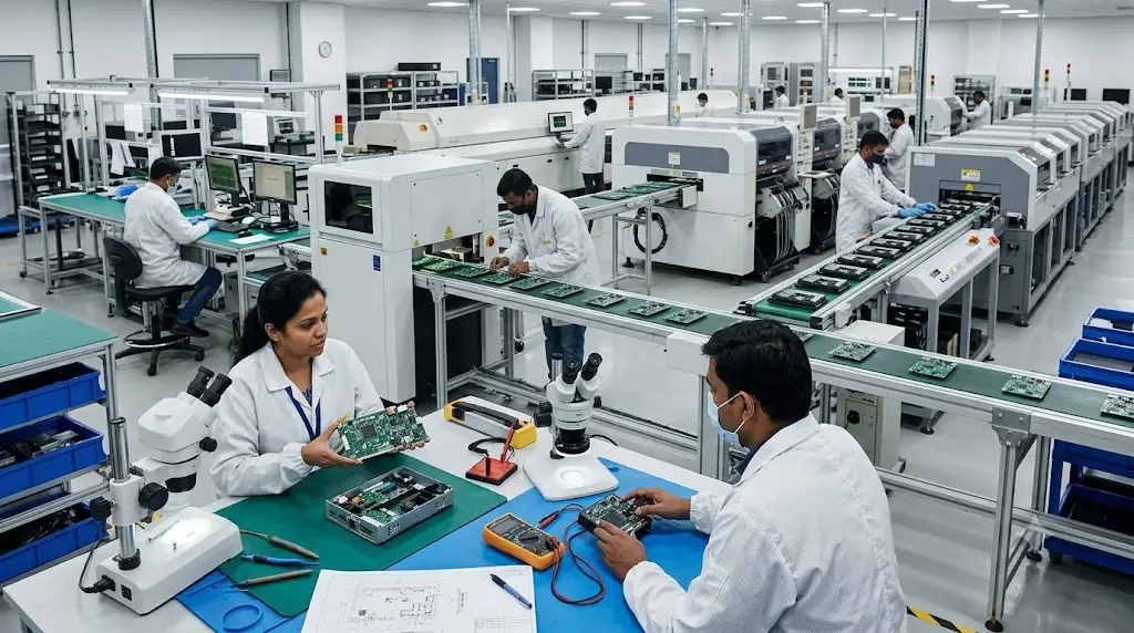
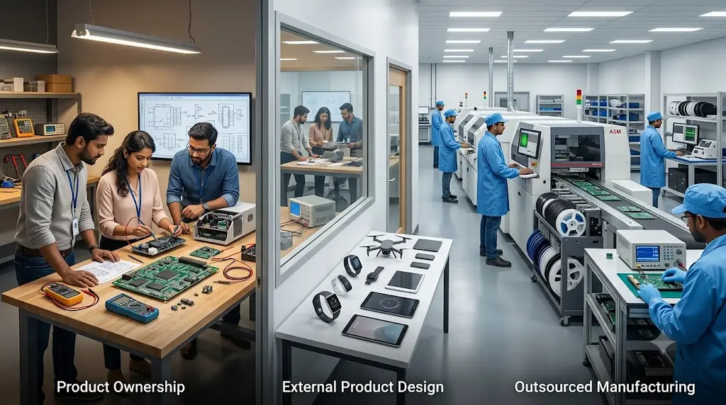
A bare printed circuit board provides the physical and electrical platform for an electronic product, but it cannot perform its intended circuit function until the required components are mounted and electrically connected. This stage is known as PCB assembly, or PCBA.
For product engineers and OEM teams, understanding the PCB assembly process is important because decisions made during assembly can affect manufacturability, board density, reliability, production speed, testing requirements and ultimately the performance of the finished electronic product.
Two of the most widely used component-mounting methods are Surface Mount Technology (SMT) and Through-Hole Technology (THT). Modern products may use one method predominantly or combine both on the same board.
This guide explains how the complete PCB assembly process works, where SMT and through-hole assembly differ, how mixed-technology boards are manufactured, and why inspection and testing should be treated as part of the process rather than as a final afterthought.
What Is PCB Assembly?
A bare printed circuit board contains the conductive tracks, pads and other physical features required to connect electronic components, but it does not yet perform the intended electronic function.
PCB assembly is the process of placing and electrically connecting components such as resistors, capacitors, integrated circuits, connectors and other devices onto that board.
Once electronic components have been mounted and soldered onto the PCB, the populated board is referred to as a printed circuit board assembly (PCBA).
This distinction is useful:
- PCB: The bare printed circuit board before electronic components are assembled.
- PCBA: The populated board after components have been mounted and soldered.
Depending on the product design, assembly may involve SMT, through-hole insertion or a combination of both.
What Are the Main Steps in the PCB Assembly Process?
The exact manufacturing flow depends on the design, component mix, production volume and testing requirements. A typical process may include:
- BOM and material verification
- PCB and manufacturing data verification
- Solder paste printing
- Surface-mount component placement
- Reflow soldering
- Inspection of the SMT assembly
- Through-hole or manual component insertion where required
- Through-hole soldering
- Visual and automated inspection
- Electrical or functional testing as required
- Final assembly, software loading and packaging where applicable
Not every board follows all these steps. For example, a board containing only surface-mount devices may not require through-hole insertion. A mixed-technology board may pass through both assembly processes.
What Is Surface Mount Technology (SMT)?
Surface Mount Technology is a PCB assembly method in which electronic components are mounted directly onto pads on the surface of the printed circuit board.
Because the component leads do not generally need to pass through drilled mounting holes, SMT supports compact board layouts and highly automated production.
It is commonly used for integrated circuits, resistors, capacitors and many other components found in modern electronics.
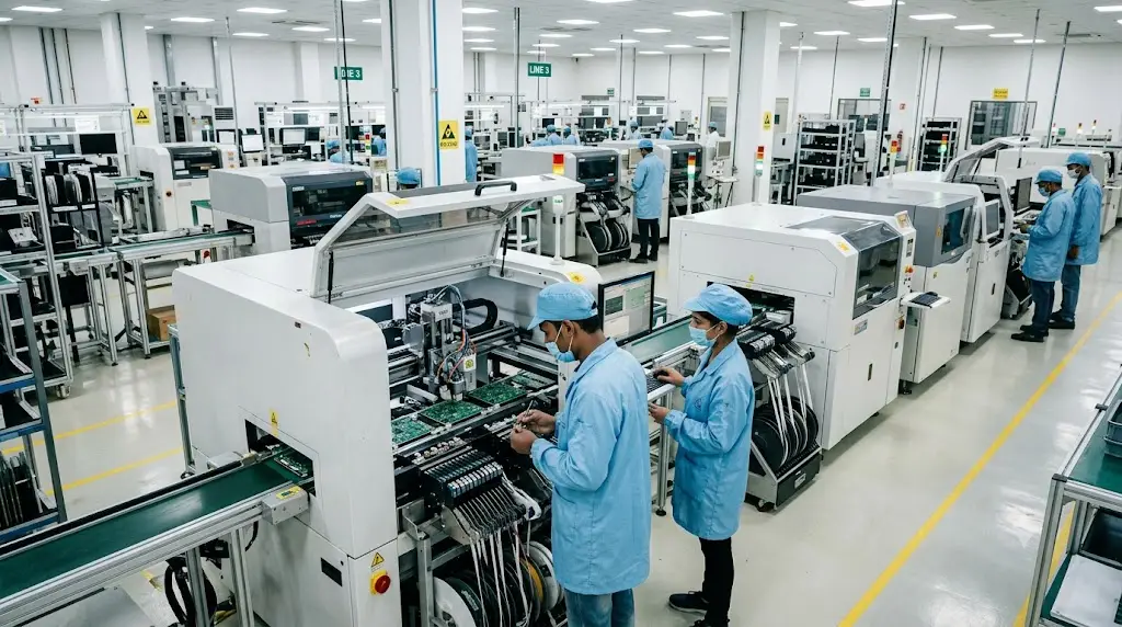
OEL’s dedicated Surface Mount Technology capabilities include automated component placement, advanced 3D solder-paste inspection and controlled reflow processes designed to support high-precision electronics manufacturing.
Step 1: Solder Paste Printing
The SMT process normally begins by applying solder paste to the required PCB pads.
A stencil aligns with the board so that paste is deposited only where surface-mount components will be soldered. Consistency at this stage matters because an incorrect amount or position of solder paste can create problems later in the assembly process.
Step 2: Solder Paste Inspection
Where the manufacturing process includes solder paste inspection, the deposited paste can be checked before components are placed.
This provides an opportunity to identify issues such as incorrect paste position or other deposition problems early in the process rather than after soldering.
Step 3: Component Placement
Automated pick-and-place machines take components from reels, trays or other feeders and position them onto the solder-paste-covered pads according to the programmed assembly data.
Automation makes SMT particularly suitable for boards containing a large number of small components or densely populated layouts.
Step 4: Reflow Soldering
After placement, the PCB moves through a reflow oven.
The board is exposed to a controlled thermal profile that heats the solder paste until reliable solder joints are formed between the components and PCB pads.
The reflow thermal profile must be controlled according to the PCB design, solder paste, component requirements and assembly process to achieve consistent solder-joint quality.
Step 5: Inspection
After reflow, the assembled board can be inspected for placement and soldering problems.
Depending on the product and manufacturing setup, inspection may include automated optical inspection, visual inspection or additional techniques for areas that cannot be evaluated easily from the board surface.
What Is Through-Hole Technology (THT)?
Through-Hole Technology uses electronic components whose leads pass through holes in the printed circuit board and are soldered on the opposite side.
The component is therefore supported not only by the solder connection but also by the lead passing through the board.
This makes through-hole assembly useful for components and applications where mechanical anchoring, component geometry or the PCB design makes surface mounting less suitable.
OEL’s Manual Insertion services address PCB assemblies where the process SOP, component requirements or uniqueness of the PCB design calls for precise manual component insertion.
Step 1: Component Insertion
Through-hole component leads are inserted into the designated plated holes in the PCB.
Depending on the product and manufacturing process, insertion can be automated, semi-automated or manual.
Manual insertion remains relevant because not every component shape, board design or assembly requirement is ideally suited to automated placement.
Step 2: Component Position Verification
Before soldering, component orientation, location and seating should be checked against the assembly requirements.
Incorrect polarity or positioning discovered at this stage is generally easier to address than after the board has completed soldering and testing.
Step 3: Soldering
Through-hole components can be soldered using different methods depending on board design, production volume and the mix of components present.
Common approaches include wave soldering, selective soldering and controlled manual soldering.
The selected method should be compatible with the PCB design and any surface-mount components already assembled on the board.
Step 4: Inspection
After soldering, the assembly should be checked for component placement and solder-joint quality according to the applicable manufacturing requirements.
SMT vs Through-Hole: What Are the Main Differences?
| Factor | SMT | Through-Hole (THT) |
| Component mounting | Components are mounted on PCB surface pads | Component leads pass through holes in the PCB |
| Automation | Highly suited to automated placement | May involve automated, semi-automated or manual insertion |
| Board density | Well suited to compact and high-density layouts | Through-holes consume additional board area and routing space |
| Component size | Supports very small surface-mount devices | Often used for larger leaded components |
| Production speed | Can support high-speed automated placement | Insertion can be slower, particularly where manual work is required |
| Mechanical anchoring | Component is soldered to surface pads | Lead passes physically through the PCB |
| Typical applications | Compact, densely populated modern electronics | Connectors, larger components and situations requiring through-hole mounting |
Is SMT Better Than Through-Hole Assembly?
Not necessarily.
SMT and THT solve different manufacturing requirements. Choosing one simply because it is newer, faster or more automated can be the wrong approach.
SMT is generally attractive when the product requires:
- High component density
- Compact PCB dimensions
- Automated high-volume assembly
- Small electronic components
- Efficient placement of large numbers of components
Through-hole assembly may be appropriate when:
- A component is designed for through-hole mounting
- Additional physical anchoring is beneficial
- The component is larger or mechanically stressed
- The PCB or process specification requires leaded insertion
- Manual assembly is required because of component or board characteristics
The correct choice therefore depends on the product rather than on a simple SMT-versus-THT preference.
What Is Mixed-Technology PCB Assembly?
Many electronic products use both surface-mount and through-hole components on the same PCB.
This is known as mixed-technology assembly.
For example, a board may use SMT for integrated circuits, resistors and other compact devices while retaining through-hole components for particular connectors or larger components.
A simplified mixed PCB assembly flow could look like this:
- Solder paste printing
- SMT component placement
- Reflow soldering
- SMT inspection
- Through-hole component insertion
- Through-hole soldering
- Final inspection
- Electrical and functional testing
The process sequence should be planned around the actual design. Manufacturing engineers need to consider component sensitivity, soldering method, thermal exposure, accessibility and inspection requirements before defining the final route.
Why PCB Inspection Matters Before Testing
Inspection and testing are related, but they are not the same thing.
Inspection looks for manufacturing or assembly conditions such as incorrect placement, missing components or visible soldering issues.
Testing evaluates whether electrical circuits, functions or the finished product behave according to the required specification.
A board can appear visually correct and still contain an electrical problem. Likewise, a defect discovered during inspection may be corrected before the board reaches functional testing.
This is why quality control is most effective when checkpoints are integrated across the manufacturing process rather than relying only on a final pass-or-fail test.
Common PCB Assembly Quality Checks
The precise inspection plan depends on the product, component packages and customer requirements. Common approaches can include the following.
Solder Paste Inspection
Solder paste inspection evaluates the paste deposited during the SMT process before component placement and reflow.
Identifying a paste-related issue early can help prevent downstream solder-joint problems.
Automated Optical Inspection
Automated optical inspection uses imaging systems to evaluate visible assembly conditions such as component presence, orientation and other detectable placement or soldering issues.
It is particularly useful in automated manufacturing environments where inspecting every populated location manually would be inefficient.
Visual Inspection
Human inspection remains useful for conditions that need contextual judgement or areas that are not easily assessed by an automated system.
This is particularly relevant in processes involving manual insertion or non-standard components.
X-ray Inspection
X-ray inspection can be used to evaluate solder joints and connections that are not directly visible, including certain bottom-terminated and area-array packages or through-hole solder conditions. Whether X-ray is required depends on the PCB design, component package and quality plan.
How Is an Assembled PCB Tested?
There is no single testing method that applies to every PCBA.
The required test strategy should be defined according to product design, critical functions, manufacturing volume, customer specifications and expected use.
Electrical Testing
Electrical checks can help identify conditions such as unintended opens, shorts or other connectivity problems depending on the test setup used for the board.
Functional Testing
Functional testing evaluates whether the assembled PCB performs the intended functions under defined test conditions.
This moves beyond checking whether components are simply present and asks whether the board behaves as designed.
Software or Firmware Loading
For certain electronic products, software or firmware may need to be loaded as part of the manufacturing and testing flow before the finished unit can be validated.
OEL’s Final Assembly, Testing and Packaging capabilities describe a process in which assembled devices move through testing and, where required, customer software flashing before final packaging.
Common PCB Assembly Problems to Watch For
Effective process control aims to detect and prevent issues before they become finished-product failures. Depending on the design and assembly method, manufacturing teams may need to watch for problems such as:
- Incorrect or missing components
- Component polarity or orientation errors
- Misalignment during placement
- Insufficient or excessive solder
- Unwanted solder connections between adjacent points
- Incomplete through-hole soldering
- Damage caused during handling or assembly
- Contamination or process-related defects
The correct prevention and inspection method depends on the actual failure mode rather than applying the same quality check to every condition.
What Should OEMs Consider When Planning PCB Assembly?
For an OEM, PCB assembly should not be evaluated only by asking whether a manufacturer has an SMT line.
A better manufacturing review includes several questions.
Does the Process Match the PCB Design?
Component packages, board density, through-hole requirements and soldering constraints should all align with available manufacturing processes.
Can the Manufacturer Handle Mixed Assemblies?
If the product includes both SMT and through-hole components, the process needs to support both without creating unnecessary production complexity.
How Is Quality Checked During Production?
Ask where inspection occurs within the line, what is checked and how detected issues are controlled.
What Testing Is Required?
The test plan should reflect the product’s real functional requirements rather than being treated as a generic final inspection step.
Can the Process Scale?
A prototype or initial production run may rely on more manual work than a mature high-volume programme. OEMs should consider how the assembly process will evolve as demand increases.
This is one reason PCB assembly should be considered within the wider electronics manufacturing process, rather than as an isolated production activity.
PCB Assembly Is a Connected Manufacturing Process
Modern PCB assembly is not simply a question of choosing SMT or through-hole technology.
It is a connected sequence involving material readiness, solder application, component placement, soldering, manual insertion where required, inspection, testing and integration into the finished product.
SMT enables compact designs and highly automated assembly. Through-hole technology remains valuable where specific components, PCB designs or mechanical requirements make leaded insertion appropriate. Many products use both.
The most reliable manufacturing approach is therefore the one built around the actual product requirements, with inspection and testing incorporated throughout the production flow.
Frequently Asked Questions
What is the PCB assembly process?
The PCB assembly process involves mounting and soldering electronic components onto a bare printed circuit board, followed by inspection and testing. Depending on the design, the process may use SMT, through-hole assembly or both.
What is the difference between PCB and PCBA?
A PCB is the bare printed circuit board. A PCBA is the board after electronic components have been mounted and soldered onto it.
What is the difference between SMT and THT?
SMT mounts components directly onto pads on the surface of a PCB, while Through-Hole Technology uses component leads that pass through holes in the board and are soldered on the opposite side.
Is SMT faster than through-hole assembly?
SMT is generally more suitable for high-speed automated component placement. Through-hole assembly may involve additional insertion and soldering steps, particularly when components require manual handling.
Can SMT and through-hole components be used on the same PCB?
Yes. Many PCB assemblies use a mixed-technology approach in which surface-mount components and through-hole components are assembled on the same board.
Why is through-hole assembly still used?
Through-hole assembly remains useful for components and PCB designs where leaded mounting, component geometry or additional physical anchoring makes it more appropriate than surface mounting.
What quality checks are used during PCB assembly?
Depending on the product and manufacturing process, quality checks may include solder paste inspection, automated optical inspection, visual inspection and appropriate inspection of connections that are not directly visible.
Is PCB inspection the same as PCB testing?
No. Inspection is primarily used to identify assembly or manufacturing conditions, while testing evaluates electrical connectivity or whether the board performs its intended functions.